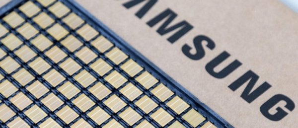

Samsung has already delivered the first shipments of HBM4 memory to its customers and announced that it has begun mass production of the new standard.
HBM4 chips are fabbed on a 6th generation of a 10nm-class DRAM process called “1c”. Note that DRAM isn’t like a CPU core, so the nodes aren’t comparable. The HBM4 products also use a 4nm logic base die for higher performance.
To put some numbers to it, HBM4 can deliver speeds of 11.7Gbps – per pin! This surpasses the industry standard, which is set at 8Gbps, by 46%. Since there are 2,048 pins the total bandwidth is a massive 3.3 terabytes per second. This is a 2.7x increase over HBM3E.
Note that when it standardized HBM4, JEDEC (the governing body for computer RAM) decided to reduce per-pin bandwidth compared to HBM3E (9.6Gbps) while doubling the number of pins from 1,024 to 2,048. This was done for improved power efficiency and better thermal management.

So, Samsung has already topped the target per-pin speed for HBM4 and surpassed the HBM3E speed. But it thinks it can do even better – it says that in the future it could build chips capable of 13Gbps per pin.
Right now, Samsung’s HBM4 memory uses a 12-layer stacking technology and is available in capacities from 24GB to 36GB. The company will adapt to the needs of its customers and could introduce a 16-layer design with up to 48GB capacity.
The Samsung-designed HBM4 memory uses low-voltage through silicon vias and a power distribution network, which improve power efficiency by 40%. Additionally, the memory stack has 10% lower heat resistance and 30% better heat dissipation compared to HBM3E.
Samsung expects to see huge demand for its memory products this year – it predicts that sales will triple compared to 2025. In anticipation of that, the company is working to expand HBM4 production capacity.

As for what comes next, next-gen HBM4E memory will be sampled to customers in the second half of 2026. Next year, it will send out custom HBM samples to customers (designed to their specifications).
“Instead of taking the conventional path of utilizing existing proven designs, Samsung took the leap and adopted the most advanced nodes like the 1c DRAM and 4nm logic process for HBM4. By leveraging our process competitiveness and design optimization, we are able to secure substantial performance headroom, enabling us to satisfy our customers’ escalating demands for higher performance, when they need them,” said Sang Joon Hwang, Executive Vice President and Head of Memory Development at Samsung Electronics.
Source